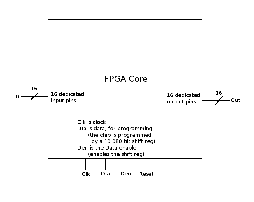
The FPGA
At the top level, The FPGA has 16 input pins, a clock pin, a reset pin, and two pins for programming.
The FPGA is programmed by a long shift register. When Den is high, at the rising edge of Clock, the value of Dta is passed into this shift register.
Once programming is done, the Reset pin is held high for a single rising Clock.
During programming, all values within the FPGA are registered, minimizing unnecessary transistor switching due to changing lookup table values. There will be more on that later.